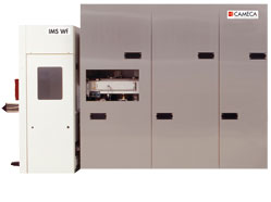
Full Wafer Magnetic Sector SIMS for Advanced Semiconductor Metrology
The CAMECA IMS Wf is a fully automated ion microprobe with benchmark performance in semiconductor ultra low energy depth profiling. It fulfills an increasing demand for fast SIMS analysis and monitoring of surface contamination in ultra shallow implants and thin layers.
Full wafer mapping & analysis capabilities
Derived from the SC Ultra (magnetic sector SIMS combining EXtreme Low Impact Energy capabilities with high mass resolution and high sensitivity), the IMS Wf adds full 300mm wafer mapping and analysis capabilities.
Wafer handling is performed by means of a robot and a shuttle designed to accommodate wafer sizes from 50 to 300 mm in diameter.
Automation and ease of use
A pattern recognition system option and a cassette to cassette loader provide the ability to perform measurements on patterned wafers. The IMS Wf therefore addresses a wide range of applications in semiconductor technology: Si, III-V compounds…
Thanks to its high level of automation, the CAMECA IMS Wf performs fast deep depth profiling with optimized sample throughput and excellent measurement stability, ensuring unequaled SIMS tool productivity.
In-depth profile through a
Multi Quantum Well structure type
semiconductor integrated laser


